CAF Voltage Divider Calculator Illustrates the Maximum Power Transfer Theorem
A Voltage Divider Calculator is the latest addition to the CAFViewer. Pat uses the calculator to illustrate the “Maximum Power Transfer Theorem” which states that an impedance-matched interface transfers the most power from a source to a load. Teaching video is included.
VDivider is a voltage divider calculator. It is the latest addition to the freeware CAFViewer Windows app. It is a playground for exploring the workings of analog audio interfaces of all types, allowing the user to develop an intuition for how these interfaces work.

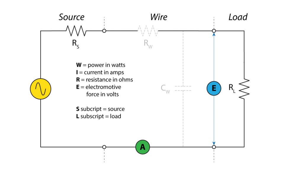
In this article, I will use VDivider to analyze the amplifier-loudspeaker interface and draw some universally applicable conclusions. First, some conventions – in this article all voltages are RMS, all impedances are resistive, and all wattages are for a continuous sine wave. Here are the conventions. Feel free to follow along in VDivider. For those of you who would rather watch a video than read an article, just skip to the end.
Optimizing for Power Transfer
The maximum power transfer theorem (and Jacobi’s Law) state that an impedance-matched interface transfers the most power from a source to a load. Under this condition, one-half of the available power from the source (WS) is delivered to the load (WL). While power transfer optimization intuitively seems like a desirable goal, especially for a power amp, it results in an efficiency of only 50%, since one-half of WS is dissipated within the source. That’s fine if you intend to cook bacon on top of your amplifier, but not if you are trying to produce sound from a loudspeaker using the minimum possible current draw from the utility circuit. Let’s use VDivide (Fig. 1) to prove the theorem.

Figure 1 – In the matched interface, RS = RL. This transfers 1/2 of the source power (WS = 60 W) to the load (WL = 30 W).
In VDivide, I have selected the Ldspk Low-Z preset and changed RS to 8 ohms, matching its impedance to the default RL = 8 Ω . The source voltage is set at 31 V, a value that conveniently produces a WS = 60 W. Note that the WL = 30 W, which is 1/2 of WS. Is it possible to get more than 30 W delivered to the load? The physics says “No” but let’s try anyway. I’ve set the source current IS to 15 A so that we don’t run out as we experiment. A good power source has more current available than is needed in actual use.

Figure 2 – Doubling the load impedance to 16 Ω reduces WL to 27 W.
If you halve the RL to 4 Ω, WL decreases to 27 W. Again, the power transfer is less than the 30 W produced by the matched condition.

Figure 3 – Halving the load impedance to 4 Ω reduces the power to the load to 27 W.
There are three important take-aways.
-
-
- 1. Maximum power transfer (50%) occurs when RL = RS. There is simply no way to get more power than the WL produced by a matched interface (30 W). This validates the maximum power transfer theorem and Jacobi’s Law. These were formalized in 1840, so this is not a new development.
- 2. When RL is increased, power transfer is reduced, but the transfer efficiency increases. With RL = 16 Ω, WS = 40 W and WL = 27 W. We are getting less WS, but more than 1/2 of it is delivered to the load (Fig. 1)! It turns out that transfer efficiency can be increased if we are willing to accept a reduction in WS. This is a BIG deal. It means we can trade away power transfer for efficiency if we are willing accept less power from the source than that produced by the impedance-matched condition. I’ll return to this later.
- 3. The voltage across the load EL is influenced by the value of RL. In this example it fluctuates between 10 V (@4 Ω) and 21 V (@16 Ω). That’s a big problem if you are driving a loudspeaker with its typical roller coaster impedance curve. Using a matched interface, it is impossible for the amplifier to preserve the shape of the input waveform at its output when driving a load with a frequency-dependent impedance (e.g. practically any real-world loudspeaker). This is the very definition of “low fidelity.”
-
Optimizing for Transfer Efficiency
Let’s repeat the exercise with some new starting values. These may seem strange at first, but stay with me.

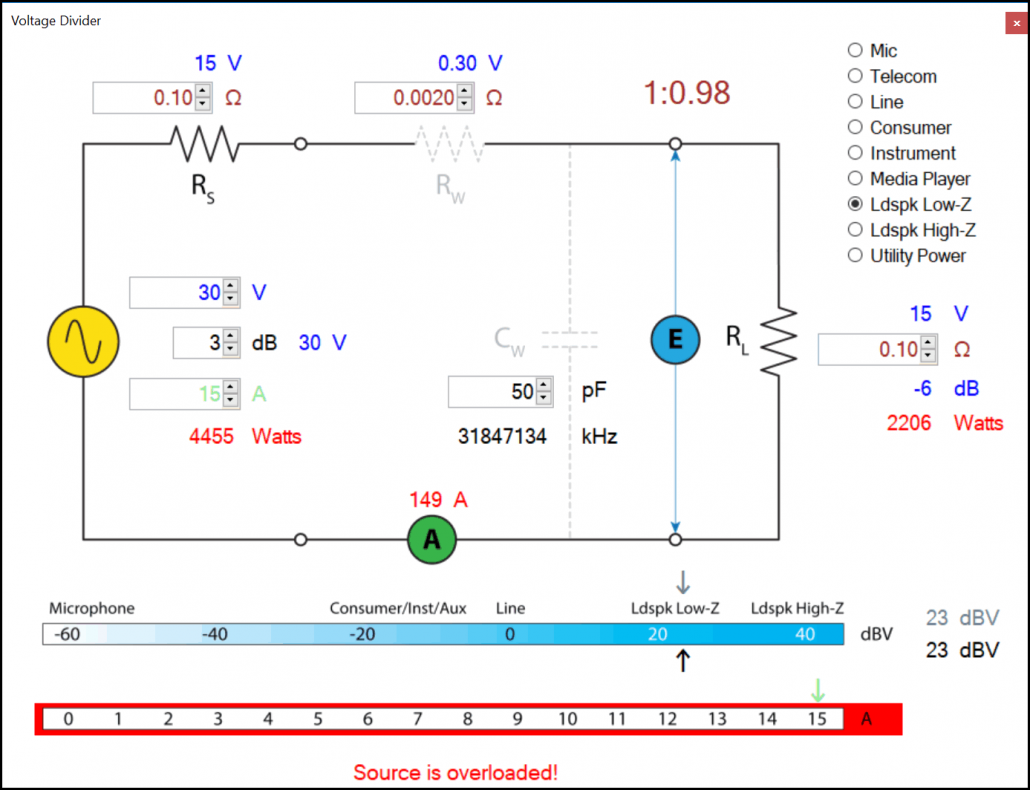
Figure 4 – A matched interface using a typical amplifier output impedance.
In the first example we found that if we are willing to accept a lower WL than produced by the matched interface, the transfer efficiency can be increased. I said that was important – here’s why.
In Fig 5 the RL is increased to 8 Ω. The WS shrinks (dramatically) to 111 W, but the transfer efficiency jumps from 50% to nearly 100%, with 110 W delivered to the load and only 1 W dissipated inside the amplifier. That’s a great trade to make, especially since this amplifier only needs to source about 4 A instead of the (theoretical) 149 A.

Figure 5 – Increasing RL to 8 Ω results in a voltage-optimized interface with nearly 100% transfer efficiency.
By optimizing for voltage transfer instead of power transfer the load voltage EL is rock solid as RL is varied. This amplifier doesn’t care what the loudspeaker’s impedance curve does.
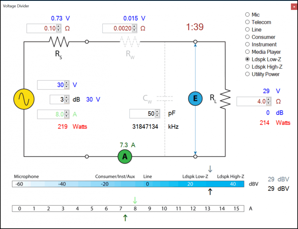
The final decision in this amplifier design is to choose a realistic source current IS. 15 A will allow a 2 ohm load to be driven by a sine wave (Fig. 6), but will also increase the size, weight, and price of the amplifier. A more modest 4 ohm rating (Fig. 7) allows IS to be reduced to about 8 A. We now have a solid 100 W @ 8 ohm amplifier that should be able to properly drive any 8 ohm loudspeaker without voltage drop. It’s a constant voltage source that delivers frequency-dependent power as determined by the loudspeaker’s impedance curve.


Figure 7 – A 4 Ω load will halve the source current requirement to about 8 A.
Conclusion
Impedance matching produces maximum power transfer from source to load. Since RS is not often specified for modern amplifiers, many assume that the amplifier-to-loudspeaker interface is matched. It is not. By making RL >> RS, the transfer efficiency is dramatically increased at the expense of achieving the maximum theoretical power transfer. This is a good trade, and one that is made by all modern solid state amplifiers.
I’ll also add that the efficiency referred to in this article is for audio power transfer to the load. The term is also used to describe the conversion of utility circuit power to audio power, which was not addressed in this article. pb
Would you rather watch than read? Here’s the video.

